Tag: Logic Gates Chart

Alternative Logic Gates | Bubbled Gates | Logic Gates

Logic Gates-


Before you go through this article, make sure that you have gone through the previous article on Logic Gates.


We have discussed-

  • Logic gates are the basic building blocks of any digital circuit.
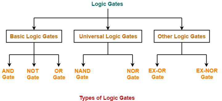
  • Logic gates are classified as-


In this article, we will discuss about Alternative Logic Gates.


Alternative Logic Gates-


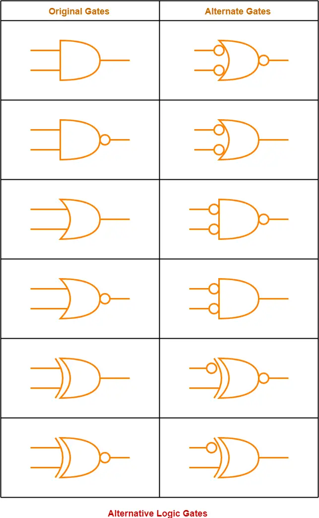
Alternative logic gate is an alternate logic gate that produces the same output as the original logic gate

and can be used during the unavailability of the original logic gate to serve the same purpose.


Alternative logic gates are also called as Alternate Gates.

Alternative logic gates are also called as Bubbled Gates since they contain bubbles in them.


The following table shows the original logic gate and its corresponding alternate gate-


Also Read- Universal Logic Gates


Rules To Memorize Alternative Logic Gates-


The following rules are helpful in drawing an alternate logic gate for a given logic gate-


For AND, NAND, OR & NOR Gates-


  • Both the inputs of alternative gate will have bubbles (which represents NOT gate).
  • For AND structured original gate, alternative gate will be OR structured.
  • For OR structured original gate, alternative gate will be AND structured.
  • If bubble is present at the output of original gate, then no bubble will be present at the output of alternative gate.
  • If bubble is not present at the output of original gate, then a bubble will be present at the output of alternative gate.


For EX-OR & EX-NOR Gates-


  • One of the inputs of alternative gate will have a bubble (which represents NOT gate).
  • For EX-OR structured original gate, alternative gate will be EX-NOR structured.
  • For EX-NOR structured original gate, alternative gate will be EX-OR structured.
  • If bubble is present at the output of original gate, then no bubble will be present at the output of alternative gate.
  • If bubble is not present at the output of original gate, then a bubble will be present at the output of alternative gate.


To gain better understanding about Alternative Logic Gates,

Watch this Video Lecture


Next Article- Latches & Flip-Flops


Get more notes and other study material of Digital Design.

Watch video lectures by visiting our YouTube channel LearnVidFun.

Universal Logic Gates | NAND Gate | NOR Gate

Logic Gates-


Before you go through this article, make sure that you have gone through the previous article on Logic Gates.


We have discussed-

  • Logic gates are the basic building blocks of any digital circuit.
  • There are 3 basic logic gates- AND, NOT, OR.
  • Logic gates are classified as-


In this article, we will discuss about Universal Logic Gates.


Universal Logic Gates-


Universal logic gates are the logic gates that are capable of implementing any Boolean function

without requiring any other type of gate.


They are called as “Universal Gates” because-

  • They can realize all the binary operations.
  • All the basic logic gates can be derived from them.


They have the following properties-

  • Universal gates are not associative in nature.
  • Universal gates are commutative in nature.


There are following two universal logic gates-


  1. NAND Gate
  2. NOR Gate


1. NAND Gate-


  • A NAND Gate is constructed by connecting a NOT Gate at the output terminal of the AND Gate.
  • The output of NAND gate is high (‘1’) if at least one of its inputs is low (‘0’).
  • The output of NAND gate is low (‘0’) if all of its inputs are high (‘1’).


Logic Symbol-


The logic symbol for NAND Gate is as shown below-


Truth Table-


The truth table for NAND Gate is as shown below-


A B Y = (A.B)’
0 0 1
0 1 1
1 0 1
1 1 0

Truth Table


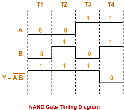
Timing Diagram-


The timing diagram for NAND Gate is as shown below-


2. NOR Gate-


  • A NOR Gate is constructed by connecting a NOT Gate at the output terminal of the OR Gate.
  • The output of OR gate is high (‘1’) if all of its inputs are low (‘0’).
  • The output of OR gate is low (‘0’) if any of its inputs is high (‘1’).


Logic Symbol-


The logic symbol for NOR Gate is as shown below-


Truth Table-


The truth table for NOR Gate is as shown below-


A B Y = A + B
0 0 1
0 1 0
1 0 0
1 1 0

Truth Table


Timing Diagram-


The timing diagram for NOR Gate is as shown below-


To gain better understanding about Universal Logic Gates,

Watch this Video Lecture


Next Article- Alternative Logic Gates


Get more notes and other study material of Digital Design.

Watch video lectures by visiting our YouTube channel LearnVidFun.

Logic Gates | Definitions | Types | Symbols | Truth Tables

Logic Gates-


Logic Gates may be defined as-


Logic gates are the digital circuits capable of performing a particular logic function

by operating on a number of binary inputs.

OR

Logic gates are the basic building blocks of any digital circuit.


Types Of Logic Gates-


Logic gates can be broadly classified as-


In this article, we will discuss about Basic Logic Gates.


Basic Logic Gates-


Basic Logic Gates are the fundamental logic gates using which universal logic gates and other logic gates are constructed.


They have the following properties-

  • Basic logic gates are associative in nature.
  • Basic logic gates are commutative in nature.


There are following three basic logic gates-

  1. AND Gate
  2. OR Gate
  3. NOT Gate


1. AND Gate-


  • The output of AND gate is high (‘1’) if all of its inputs are high (‘1’).
  • The output of AND gate is low (‘0’) if any one of its inputs is low (‘0’).


Logic Symbol-


The logic symbol for AND Gate is as shown below-


Truth Table-


The truth table for AND Gate is as shown below-


A B Y = A.B
0 0 0
0 1 0
1 0 0
1 1 1

Truth Table


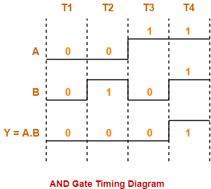
Timing Diagram-


The timing diagram for AND Gate is as shown below-


2. OR Gate-


  • The output of OR gate is high (‘1’) if any one of its inputs is high (‘1’).
  • The output of OR gate is low (‘0’) if all of its inputs are low (‘0’).


Logic Symbol-


The logic symbol for OR Gate is as shown below-


Truth Table-


The truth table for OR Gate is as shown below-


A B Y = A + B
0 0 0
0 1 1
1 0 1
1 1 1

Truth Table


Timing Diagram-


The timing diagram for OR Gate is as shown below-


Also Read- Alternative Logic Gates


3. NOT Gate-


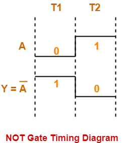
  • The output of NOT gate is high (‘1’) if its input is low (‘0’).
  • The output of NOT gate is low (‘0’) if its input is high (‘1’).


From here-

  • It is clear that NOT gate simply inverts the given input.
  • Since NOT gate simply inverts the given input, therefore it is also known as Inverter Gate.


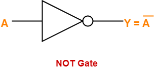
Logic Symbol-


The logic symbol for NOT Gate is as shown below-


Truth Table-


The truth table for NOT Gate is as shown below-


A Y = A’
0 1
1 0

Truth Table


Timing Diagram-


The timing diagram for NOT Gate is as shown below-


To gain better understanding about Logic Gates,

Watch this Video Lecture


Next Article- Universal Logic Gates


Get more notes and other study material of Digital Design.

Watch video lectures by visiting our YouTube channel LearnVidFun.