Half Adder-
- Half Adder is a combinational logic circuit.
- It is used for the purpose of adding two single bit numbers.
- It contains 2 inputs and 2 outputs (sum and carry).

Half Adder Designing-
Half adder is designed in the following steps-
Step-01:
Identify the input and output variables-
- Input variables = A, B (either 0 or 1)
- Output variables = S, C where S = Sum and C = Carry
Step-02:
Draw the truth table-
| Inputs | Outputs | ||
| A | B | C (Carry) | S (Sum) |
| 0 | 0 | 0 | 0 |
| 0 | 1 | 0 | 1 |
| 1 | 0 | 0 | 1 |
| 1 | 1 | 1 | 0 |
Truth Table
Step-03:
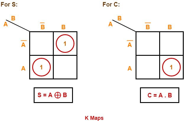
Draw K-maps using the above truth table and determine the simplified Boolean expressions-

Also Read- Half Subtractor
Step-04:
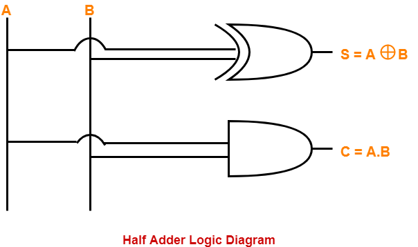
Draw the logic diagram.
The implementation of half adder using 1 XOR gate and 1 AND gate is as shown below-

Limitation of Half Adder-
- Half adders have no scope of adding the carry bit resulting from the addition of previous bits.
- This is a major drawback of half adders.
- This is because real time scenarios involve adding the multiple number of bits which can not be accomplished using half adders.
To overcome this drawback, Full Adder comes into play.
To gain better understanding about Half Adder,
Next Article- Full Adder
Get more notes and other study material of Digital Design.
Watch video lectures by visiting our YouTube channel LearnVidFun.