Ripple Carry Adder-
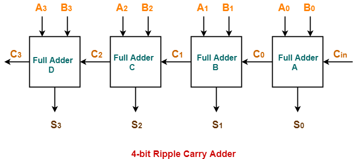
Before you go through this article, make sure that you have gone through the previous article on Ripple Carry Adder.
We have discussed-
- Ripple Carry Adder is a combinational logic circuit.
- It is used for the purpose of adding two n-bit binary numbers.
- It is also called as n-bit parallel adder.

In this article, we will discuss about Delay in Ripple Carry Adder.
Delay in Ripple Carry Adder-
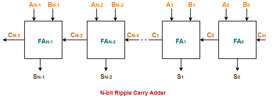
Consider a N-bit Ripple Carry Adder as shown-
The following kinds of problems may be asked based on delay calculation in Ripple Carry Adder.
Type-01 Problem:
- You will be given the carry propagation delay and sum propagation delay of each full adder.
- You will be asked to calculate the worst case delay of the ripple carry adder.
Solution-
Know These Terms?
It is important to know the following terms-
|
In Ripple Carry Adder,
- A full adder becomes active only when its carry in is made available by its adjacent less significant full adder.
- When carry in becomes available to the full adder, it starts its operation.
- It produces the corresponding output sum bit and carry bit.
If you are asked to calculate the time after which the output sum bit or carry bit becomes available from any particular full adder, then it is calculated as-
Time After Which Carry Bit Cx Becomes Available-
Required time
= Total number of full adders till full adder producing Cx X Carry propagation delay of full adder
Time After Which Sum Bit Sx Becomes Available-
Required time
= Time taken for its carry in to become available + Sum propagation delay of full adder
= { Total number of full adders before full adder producing Sx X Carry propagation delay of full adder } + Sum propagation delay of full adder
We will calculate worst case delay for the last full adder.
Also Read- Full Adder
Type-02 Problem:
- You will be given the propagation delay of some basic logic gates.
- You will be told how the full adder has been implemented.
- Then, you will be asked to calculate the worst case delay of Ripple Carry Adder.
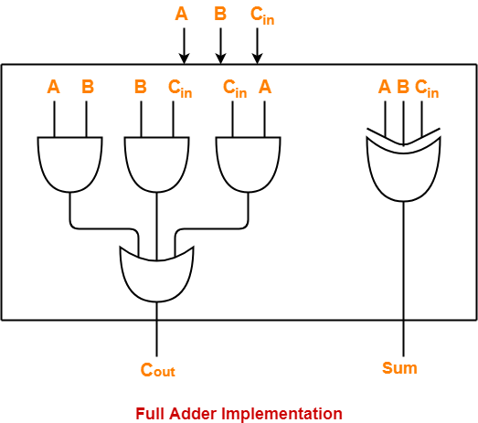
Suppose each full adder in the given ripple carry adder has been implemented as-

Solution-
- The computation has to be done in the same manner as in Type-01 problem.
- It’s just that in Type-02 problem, one step is increased.
- We have to first calculate the carry propagation delay and sum propagation delay in terms of logic gates.
- Then, our problem will reduce to Type-01 problem.
Let-
- Propagation delay of AND gate = Tpd (AND)
- Propagation delay of OR gate = Tpd (OR)
- Propagation delay of XOR gate = Tpd (XOR)
Calculating Carry Propagation Delay-
- We calculate the carry propagation delay of full adder using its carry generator logic circuit.
- It has 2 levels in the given implementation.
- At first level, three AND gates operate.
- All the three AND gates operate in parallel.
- So, we consider the propagation delay due to only one AND gate.
- At second level, OR gate operates.
Now,
Carry propagation delay of full adder
= Time taken by it to generate the output carry bit
= Propagation delay of AND gate + Propagation delay of OR gate
= Tpd (AND) + Tpd (OR)
Calculating Sum Propagation Delay-
- We calculate the sum propagation delay of full adder using its sum generator logic circuit.
- It has only 1 level at which XOR gate operates in the given implementation.
Now,
Sum propagation delay of full adder
= Time taken by it to generate the output sum bit
= Propagation delay of XOR gate
= Tpd (XOR)
Now,
- We have got the carry propagation delay and sum propagation delay of full adders.
- Our problem reduces to Type-01 problem.
- We use the same formulas as we have learnt in Type-01 problem to make the required calculations.
NOTE-
Consider in the question,
- It was said that while implementing the sum generator logic circuit of full adders, only 2-input XOR gates are used.
- Then, in that case we would require two such XOR gates which would work at 2 levels.
- So, in that case, sum propagation delay would be twice the propagation delay of XOR gate.
PRACTICE PROBLEMS BASED ON RIPPLE CARRY ADDER DELAY CALCULATION-
Problem-01:
A 16-bit ripple carry adder is realized using 16 identical full adders. The carry propagation delay of each full adder is 12 ns and the sum propagation delay of each full adder is 15 ns. The worst case delay of this 16 bit adder will be ______?
A) 195 ns
B) 220 ns
C) 250 ns
D) 300 ns
Solution-
We consider the last full adder for worst case delay.
Time after which output carry bit becomes available from the last full adder
= Total number of full adders X Carry propagation delay of full adder
= 16 x 12 ns
= 192 ns
Time after which output sum bit becomes available from the last full adder
= Time taken for its carry in to become available + Sum propagation delay of full adder
= { Total number of full adders before last full adder X Carry propagation delay of full adder } + Sum propagation delay of full adder
= { 15 x 12 ns } + 15 ns
= 195 ns
Thus, Option (A) is correct.
For more explanation, Watch this Video Solution.
Problem-02:
Following figure shows the implementation of full adders in a 16-bit ripple carry adder realized using 16 identical full adders. The propagation delay of the XOR, AND and OR gates are 20 ns, 15 ns and 10 ns respectively. The worst case delay of this 16 bit adder will be ______?
A) 395 ns
B) 220 ns
C) 400 ns
D) 300 ns

Solution-
We consider the last full adder for worst case delay.
Time after which output carry bit becomes available from the last full adder
= Total number of full adders X Carry propagation delay of full adder
= Total number of full adders X { Propagation delay of AND gate + Propagation delay of OR gate }
= 16 x { 15 ns + 10 ns }
= 16 x 25 ns
= 400 ns
Time after which output sum bit becomes available from the last full adder
= Time taken for its carry in to become available + Sum propagation delay of full adder
= { Total number of full adders before last full adder X Carry propagation delay of full adder } + Propagation delay of XOR gate
= { 15 x (15 ns + 10 ns) } + 20 ns
= 395 ns
Thus, Option (C) is correct.
To gain better understanding about Delay in Ripple Carry Adder,
Next Article- Carry Look Ahead Adder
Get more notes and other study material of Digital Design.
Watch video lectures by visiting our YouTube channel LearnVidFun.
